Eindhoven researchers present revolutionary light-emitting silicon: big step forward in production of photonic chips

That photonic chips have considerable advantages over electronic chips was already well known. Data transfer can take place faster and more cheaply and, moreover, without the heat production that large data centers now suffer from. Until now, however, this could not be done using silicon (sand) as a raw material; the much more expensive and rare gallium arsenide and indium phosphide had to be used for it. However, researchers at the Eindhoven University of Technology (TU/e) have now discovered a way to still emit light with silicon. It’s a breakthrough after 50 years of research.
Emitting light from silicon has been the ‘Holy Grail’ in the microelectronics industry for decades. Researchers from the Eindhoven University of Technology, together with colleagues from the universities of Jena, Linz, and Munich, now succeeded in doing just that: they have developed an alloy with silicon that can emit light. The results have been published in the journal Nature. The team will now start creating a silicon laser to be integrated into current chips.


Every year we use and produce significantly more data. But our current technology, based on electronic chips, is reaching its ceiling. The limiting factor is heat, resulting from the resistance that the electrons experience when traveling through the copper lines connecting the many transistors on a chip. If we want to continue transferring more and more data every year, we need a new technique that does not produce heat. Bring in photonics, which uses photons (light particles) to transfer data.
In contrast to electrons, photons do not experience resistance. As they have no mass or charge, they will scatter less within the material they travel through, and therefore no heat is produced. The energy consumption will, therefore, be reduced. Moreover, by replacing electrical communication within a chip by optical communication, the speed of on-chip and chip-to-chip communication can be increased by a factor 1000. Data centers would benefit most, with faster data transfer and less energy usage for their cooling system. But these photonic chips will also bring new applications within reach. Think of laser-based radar for self-driving cars and chemical sensors for medical diagnosis or for measuring air and food quality.
Laser beams
To use light in chips, you will need a light source; an integrated laser. The main semiconductor material that computer chips are made of is silicon. But bulk silicon is extremely inefficient at emitting light, and so was long thought to play no role in photonics. Thus, scientists turned to more complex semiconductors, such as gallium arsenide and indium phosphide. These are good at emitting light but are more expensive than silicon and are hard to integrate into existing silicon microchips.
To create a silicon compatible laser, scientists needed to produce a form of silicon that can emit light. That’s exactly what the researchers now succeeded in. They combined silicon and germanium in a hexagonal structure that is able to emit light.


“The crux is in the nature of the so-called band-gap of a semiconductor,” says lead researcher Erik Bakkers from TU/e. “If an electron ‘drops’ from the conduction band to the valence band, a semiconductor emits a photon: light.” But if the conduction band and valence band are displaced with respect to each other, which is called an indirect band-gap, no photons can be emitted – as is the case in silicon. “A 50-year old theory showed however that silicon, alloyed with germanium, shaped in a hexagonal structure does have a direct band-gap, and therefore potentially could emit light,” says Bakkers.
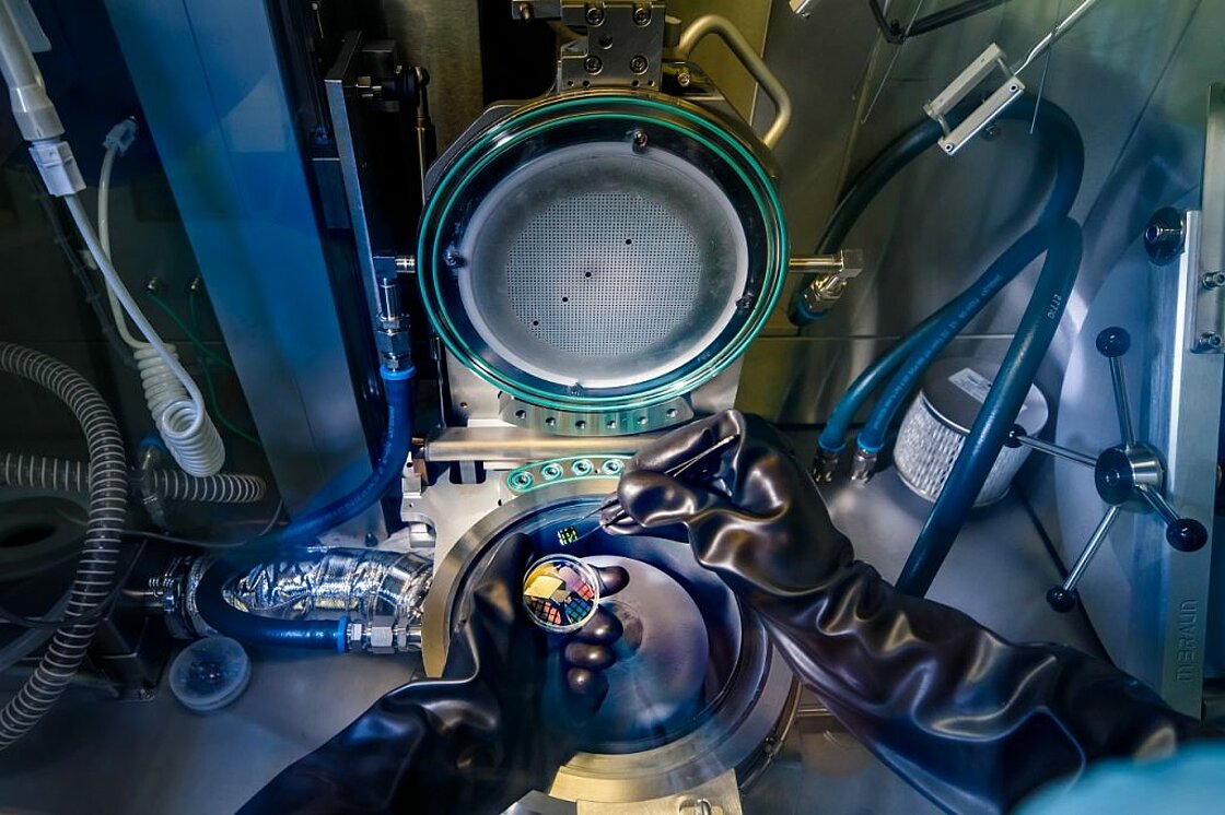
Shaping silicon in a hexagonal structure, however, is not easy. As Bakkers and his team master the technique of growing nanowires, they were able to create hexagonal silicon in 2015. They realized pure hexagonal silicon by first growing nanowires made from another material, with a hexagonal crystal structure. Then they grew a silicon-germanium shell on this template. Elham Fadaly, shared first author of the Nature paper: “We were able to do this such that the silicon atoms are built on the hexagonal template, and by this forced the silicon atoms to grow in the hexagonal structure.”
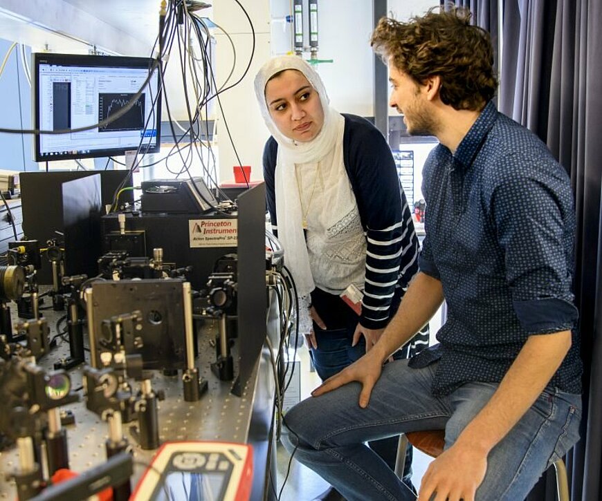
But they could not yet make them emit light, until now. Bakkers’ team managed to increase the quality of the hexagonal silicon-germanium shells by reducing the number of impurities and crystal defects. When exciting the nanowire with a laser, they could measure the efficiency of the new material. Alain Dijkstra, also shared first author of the paper and responsible for measuring the light emission: “Our experiments showed that the material has the right structure and that it is free of defects. It emits light very efficiently.”
Creating a laser now is a matter of time, Bakkers thinks. “By now we have realized optical properties which are almost comparable to indium phosphide and gallium arsenide, and the material’s quality is steeply improving. If things run smoothly, we can create a silicon-based laser in 2020. This would enable tight integration of optical functionality in the dominant electronics platform, which would break open prospects for on-chip optical communication and affordable chemical sensors based on spectroscopy.”
Article by Innovation Origins