TNO at Holst Centre Set to Revolutionise Microelectronic Manufacturing with Novel Printing Solution
As electronics simultaneously become smaller and more powerful, manufacturers are seeking ways to accelerate and scale the production of microelectronic devices. For this reason, TNO at Holst Centre announces the solution: and it offers acceleration at a speed with more than 1 million G-forces. The proprietary Impulse PrintingTM technique addresses key manufacturing challenges, at a mere fraction of the cost.

Impulse Printing enables the precise, scalable and sustainable production of semiconductors, circuit boards and displays – including micoLED displays – essential for modern devices. All with a lower cost of ownership and higher throughput.
How it works
Impulse PrintingTM is a new type of additive manufacturing technology. It transfers high-resolution patterns using rapid surface heating. When the solvent at the heated interface reaches its boiling temperature, rapid gas generation leads to pressure build-up. This pressure causes the ink to accelerate with more than 1 million G-forces, and transfer to the substrate.
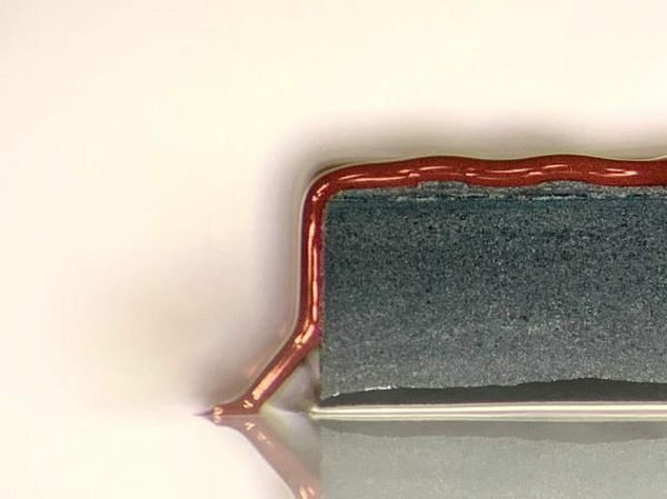
This precise and easy-to-use technique addresses many manufacturing challenges. It can deposit feature sizes ranging from several microns to many millimetres. The ink does not experience any shear forces, which means a wide range of viscosities can be deposited. Impulse Printing can therefore print on any type of surface, and with even the most highly viscous inks. Patterns can even be printed over gaps, on steps, or wrapped around substrates.
Targeted improvement on state-of-the-art
Currently, manufacturers employ techniques like lithography or dispensing to create the intricate components that make up modern devices. But as Rob Hendriks, Program Lead at TNO at Holst Centre explains, these techniques come with challenges. ‘Lithography is scalable, so is conducive to mass production. But it cannot create the essential 3D interconnects for hybrid electronic components the way Impulse Printing can. What’s more, lithography generates a great deal of waste, so the solution isn’t very sustainable in the long term. In contrast, dispensing is both sustainable and capable of creating 3D interconnects. But scaling the solution for mass production isn’t possible.’

Industry-ready
‘Impulse Printing is a non-contact and high-throughput technology,’ explains Hendriks. ‘It can easily be integrated into current manufacturing set-ups, including roll-to-roll processes. And manufacturers can print microelectronic features – including 3D interconnects – with the simple push of a button.’
In addition, Impulse Printing has a much lower cost of ownership, because it requires only 1% of the facility space of traditional techniques, and is more than 10 times more cost-effective. And because of efficient use of materials, the solution is more sustainable than traditional techniques.
Demonstration and further development
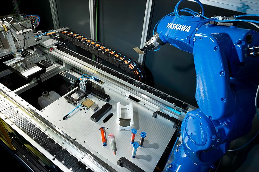
The revolutionary Impulse Printing solution is demonstrated at Holst Centre’s office at the High Tech Campus. There, the capabilities of the technology and the speed and accuracy of the techniques will be on full display.
TNO at Holst Centre will continue to develop the technology, together with industry partners who can test any solution and any substrate on the proto-tool available at Holst Centre. At the same time, the current technology is preparing for market availability through a spin-off company. For more information, please contact Rob Hendriks.