SCIL-Nanoimprint Solutions enables mass production of nanostructures

Using patented lithography technology, SCIL Nanoimprint Solutions (SCIL-Nano) offers cutting-edge solutions for patterning nanostructures on large wafers.
The journey began in 2015 at Philips Research, where Remco van Brakel (CCO), Rob Voorkamp (CEO), and Marc Verschuuren (CTO) were working on developing SCIL (Substrate Conformal Imprint Lithography). With Philips’ support, they decided to take the plunge and build a business around this innovative technology. As of the end of this year, SCIL-Nano stands independently, having secured a €10 million investment. We spoke with CEO Rob Voorkamp about their exciting journey and future plans.
What does SCIL-Nanoimprint Solutions do?
'SCIL or Substrate Conformal Imprint Lithography is a cost-effective, robust high, yield process that enables nanometer resolution patterning on a wide variety of materials. SCIL delivers proven high-quality prints on wafer surfaces up to 300 mm.
Our customers use this technology to create high-resolution, cost-effective, scalable, versatile, and reliable patterns for various high-tech components. These can be lenses and other photonics components used in smart glasses, cell phones, sensors, and semiconductors. With SCIL, our customers can ultimately drive innovation and maintain a competitive market advantage.'
What is the advantage of SCIL technology?
'With optical lithography, you have problems focusing on a flat surface. SCIL technology does have the ability to apply nanostructures to surfaces that are not entirely flat. Think of lasers or LEDs and almost all applications where you want to use a structure to glass, but also semiconductors where many layers have already been applied.
In addition, we can apply complex (3D) structures with different materials in one pass, structures on two sides of a glass wafer, and our machines and processes are often cheaper than DUV tools and use up to 80% less energy.
But there are drawbacks, too. We are good at making very accurate (10 nm resolution) structures. Still, if we need to apply a second layer, we can align it at about 0.5 micrometers relative to the first layer. This needs to be better for semiconductors’ first layers (front-end). So, we are not competing with EUV. So we mainly focus on photonic applications and back-end semicon.'
What is the ultimate goal?
'We provide machines, consumables, and process support to enable our customers to produce their products cost-effectively and scalably. Our goal is to be the partner of choice for any company that wants to improve its products by applying nanostructures. In doing so, we want to support the customer from design to sample production to volume production.'
What was the biggest challenge?
'Defining the right business model. For us, that provided production machines and recurring revenue from the consumables that products need to run their production.'
And the most significant success?
'We have three major customers using our machines for the volume production of lasers and augmented reality lenses. The last customer has built a complete production line from scratch around our technology for producing waveguides.'
Advantage of the Brainport eco system
'Because we’re a Philips spin-off, it was logical to develop our start-up in the Brainport region. We work a lot with all kinds of companies in Brainport. For example, VDL-ETG makes our imprint machines. However, the ecosystem should work on better, more affordable, and flexible infrastructure facilities, such as clean rooms and laboratories.'
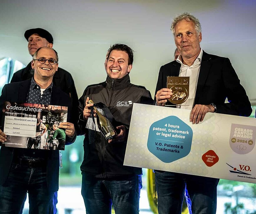
The Gerard & Anton Awards are supported by EY, Rabobank, V.O. Patents & Trademarks, TWICE, Kadans Science Partner, Braventure, Lumo Labs, Gemeente Eindhoven, High Tech Campus, Philips, Goevaers & Znn. B.V. and DeepTechXL.

