EFFECT Photonics

Technology
Dense Wavelength Division Multiplexing crucial for development integrated optical chips
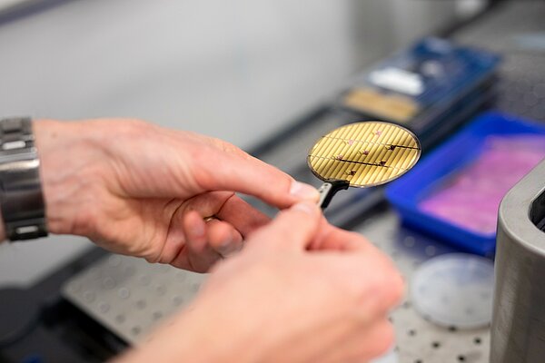
EFFECT Photonics develops highly integrated optical chips based on its Dense Wavelength Division Multiplexing (DWDM) optical System-on-Chip technology. The chips guide light instead of electrons and are based on InP (Indium Phosphide), a material that enables creating efficient laser light sources, waveguides, modulators, and photodiodes used in optical communication systems throughout the world. In the development of fibre optic transmission technology, the emergence of Dense Wavelength Division Multiplexing (DWDM) has been one of the most important and innovative developments.
Combine all functions on single chip
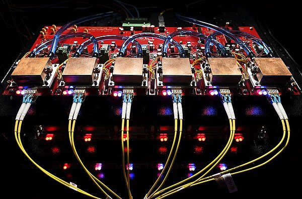
DWDM makes it possible to combine all photonic components and functions within a single chip. This, combined with simple packaging, makes it possible to produce these chips in volume with high yield at low cost. With this capability, EFFECT Photonics is addressing the need for low-cost DWDM solutions particularly for meeting the demand for high bandwidth connections between data centers and back from mobile cell towers making it possible to deliver more data through existing fiber.
A platform approach
EFFECT Photonics takes a platform approach to integration using high-yielding building blocks within the wafer. Growing different quaternary alloys of Indium Phosphide on a single wafer means that all of the active and passive optical functions of a system can be created within a single chip. All of the building blocks are developed and described in such a way that it can easily be used for purposes other than telecom.
Talent
‘Realising the seemingly impossible’
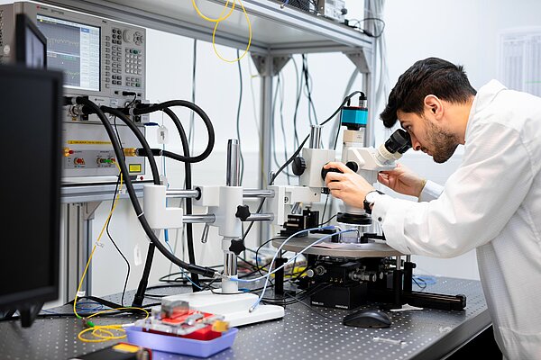
Jeffrey Lee is Senior Product Architect at EFFECT Photonics where he and his team work on high-quality lasers integrated on a single photonic chip at low power and costs, enabling wide adoption of next-generation optical communication systems. What drives him most is the enormous complexity of the technology he works on and the fact that he is making things possible that have never been possible before. “A multitude of technological advances such as electronics, signal processing, integrated photonics, packaging, manufacturing, as well as factors such as infrastructure, talent, and investment needed to come together simultaneously to make this happen.”
Delivering more data through existing fiber
“I studied in Eindhoven, did my Ph.D. in optical communications and lived in Munich for eight years, after that, I lived in the US for eight years. When I was doing my Ph.D., integrated photonics were just at the beginning of breaking through. The many benefits integrated photonics offer is what drove the research. It is a great moment to be working on this technology now. What we try to do is deliver more data through existing fiber, we do this by modulating the light in multiple dimensions and combining all of these functions on a single platform.”
Room for experiment
After living in the US, I realized that what I really like about Europe is the excellent work-life balance and the fact that you can take risks without severe consequences here. There is a good social support system that you can fall back on, which gives you a lot of freedom to try new things. It surprises me that people here don’t take more risks and start many more innovative businesses to compete with the US. You really have the chance to experiment and realize your ideas here.
We are doing it together
Within EFFECT Photonics I get the opportunity to work on many things. The company culture is open and transparent. You know exactly where you stand. It is really an international company with a good mix of males and females from many different countries working together. Working at a start-up like EFFECT Photonics is great: you have a lot of responsibility, you need multiple skills and you need to combine all of those skills to make it work. Here, we are like a family, we are doing it together.”

Societal impact
Unlimited data transmission capacity and bandwidth
The need for data grows with 50% per year and highspeed communication is going to be crucial to enable the next generation of technology such as 5G, IoT, connected and automated mobility and more. The ability to provide the world with potentially unlimited data transmission capacity and bandwidth, therefore, is a massive advantage of EFFECT Photonics’ DWDM technology. Moreover, it makes it possible to transport more data, using the same amount of energy.
Fast, affordable, effective and sustainable
EFFECT Photonics is shaping the future by interconnecting humanity through fast, affordable, sustainable, and effective communication technologies. From both technical and economic perspectives, the ability to provide the world with potentially unlimited data transmission capacity and bandwidth is key to enabling technological and societal progress.
Brainport factor
Turning Science into disruptive technology
About 160 photonics companies are situated in the Netherlands and the center of gravity lies in the Brainport Eindhoven region. It is an important worldwide hub for integrated photonics, embodied by The Photon Delta ecosystem, which is the sum of high-tech companies, knowledge institutions and authorities that have joined forces to gain a leading position in the development of photonics. Today Brainport Eindhoven not only provides access to worldwide scientific knowledge and research facilities in the field of optics, but it is also one of the first regions that is about to turn this ground-breaking technology into business. This makes it an extremely attractive place to be for engineers.
Brainport attractive to tech talent
Brainport Eindhoven is also a good place to be located from a talent perspective. As the roots of EFFECT Photonics lie in Eindhoven University of Technology it helped to attract the talent needed for starting up the company. Moreover, the city of Eindhoven has a good reputation among engineers and a vivid international community where you can feel the tech vibe and find a lot of tech and IT companies in all sorts and sizes.